ภาพความเสียหายที่เกิด จาก ESD
Posted 6 Jul 2018 11:30 | 5,178 views
รวบรวม ภาพความเสียหาย จากการเกิดไฟฟ้าสถิต ESD ไหลลงวงจร โดยScanning Electron Micrograph (SEM) defect ต่างๆที่เกิดขึ้นนั้นไม่สามารถมองเห็นด้วยตาเปล่า ต้องใช้เครื่องมือเฉพาะทางเพื่อตรวจสอบเท่านั้น ปัญหา ESD หรือ EOS เหมือนภูเขาน้ำแข็งเมื่อเกิดขึ้นแล้วต้นทุนที่จะแก้ไขมหาศาล ไม่อาจประเมินได้ ดังนั้นต้องควบคุมกระบวนการผลิต และการตรวจสอบให้ถูกต้อง สำหรับเครื่องมือนั้นเราแนะนำให้ใช้ DESCO ซึ่งได้รับการยอมรับจากสากล ท่านสามารถติดต่อเราเพื่อนำเครื่องมือ DESCO ไปทดสอบได้
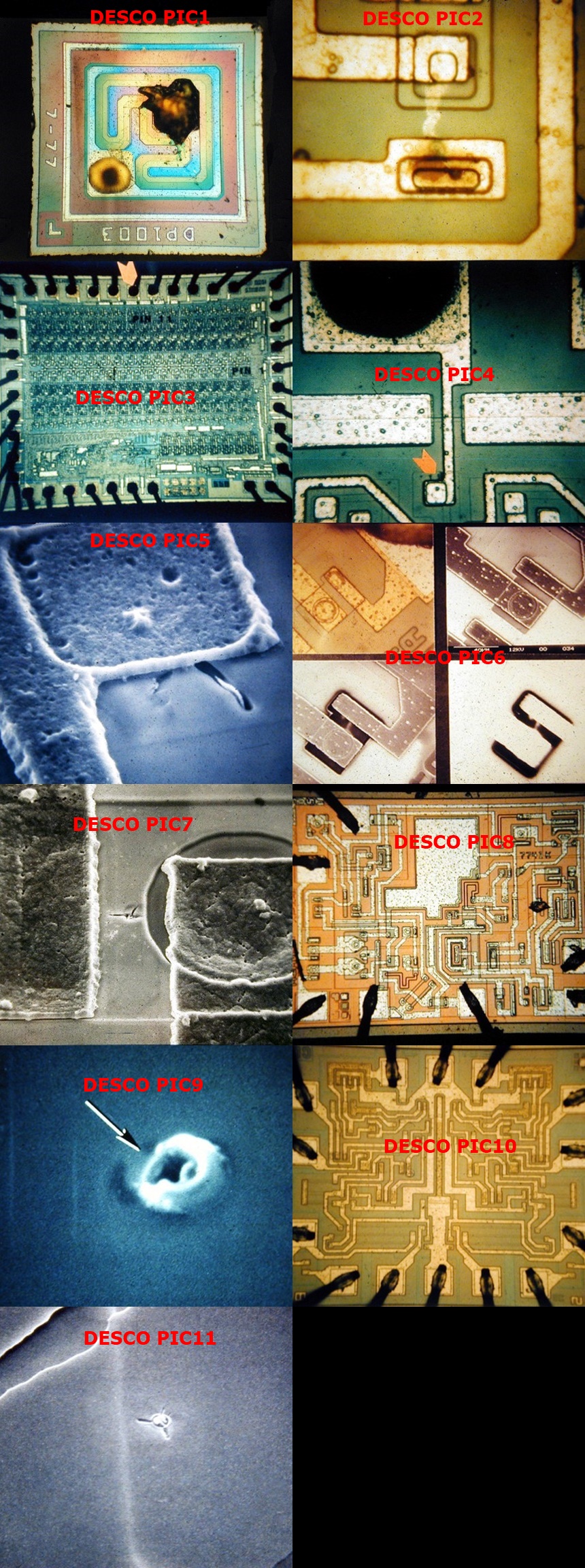
Picture 1 This is not HBM-ESD. Extensive damage on this transistor where the bond has melted is typical of surges from Inductors, Transformers, and Motors.
Picture 2 Arcing of this nature within an integrated circuit is typical of testing damage. Human Body Model ESD does not create sufficient damage to be seen in an optical microscope
Picture 3 Optical photo of a large Integrated Circuit which has experienced ESD damage to the pin noted by the arrow
Picture 4 Higher magnification photo of pin noted by the arrow in the prior slide This taken at 400 times magnification on a 4" X 5" photo. The damage is noted as the "fuzz" at the end of the arrow..
Picture 5 Now you see it!! Overlying glaciation has been removed and the surface decorated to show the ESD damage at 5,000 times magnification in this scanning electron micrograph
Picture 6 Techniques used to locate HBM-ESD damage in an integrated circuit. Clockwise from the upper left optical photo at 400X shows no damage. The upper right hand scanning electron micrograph (SEM) shows no damage. The lower right hand image is the current flow in the device
which shows a subsurface arc between the two metal lines. The lower left photo is a combination of the SEM image and the current flow image.
which shows a subsurface arc between the two metal lines. The lower left photo is a combination of the SEM image and the current flow image.
Picture 7 Scanning electron micrograph (SEM) image of the device in prior slide after glassivation removal and surface decoration. The enlargement 2,000 times magnification.
Picture 8 Optical micrograph of an Integrated Circuit damaged by HBM ESD. Damage has occurred in the large thin oxide metal capacitor in the upper center of the image. However, no physical damage is visible
Picture 9 Scanning electron micrograph (SEM) image of the ESD damage after removal of the capacitor metallization. Note the characteristic eruption thru the oxide. Magnification is 10,500 times.
Picture 10 Optical image of an Integrated Circuit damaged by HBM ESD. The second pin from the bottom left is good and its mirror image, second from the right is damaged. However, no physical damage is visible.
Picture 11 Scanning electron micrograph (SEM image of the damage site on the Integrated Circuit shown in prior slide. Metal has been removed expose the underlying damage site. Magnification is 6,450 times.
ภาพทุกใบเป็น COPY RIGHT DESCO ถ้าต้องการนำไปใช้เพื่อการศึกษาหรือเผยแพร่ขอให้แจ้งกลับบริษํท มอสโทริ จำกัด